MMX™ Technology Developers Guide
Information for Developers and ISVs From Intel® Developer Services www.intel.com/IDS

MMX™ Technology Developers Guide
Information for Developers and ISVs From Intel® Developer Services www.intel.com/IDS
Subject to the terms and conditions set forth below, Intel hereby grants you a nonexclusive, nontransferable license, under its patents and copyrights on the example code sequences contained in the IA MMX™ Technology Developer's Manual, to use, reproduce and distribute such example code sequences, solely as part of your computer program(s) and solely in order to allow your computer program(s) to implement the multimedia instructions contained in such sequences solely with respect to the Intel instruction set architecture. No other license, express, implied, statutory, by estoppel or otherwise, to any other intellectual property rights is granted herein. THIS DOCUMENT AND ALL INFORMATION, PROPOSALS, SAMPLES AND OTHER MATERIALS PROVIDED IN CONNECTION WITH OR IN RELATION TO THIS DOCUMENT (INCLUDING, WITHOUT LIMITATION, THE EXAMPLE CODE SEQUENCES) ARE PROVIDED "AS IS" WITH NO WARRANTIES, EXPRESS, IMPLIED, STATUTORY OR OTHERWISE, AND INTEL SPECIFICALLY DISCLAIMS ANY IMPLIED WARRANTY OF MERCHANTABILITY, NONINFRINGEMENT OR FITNESS FOR ANY PARTICULAR PURPOSE. Any use or distribution of this document or the materials contained herein must fully comply with all then current laws of the United States including, without limitation, rules and regulations of the United States Office of Export Administration and other applicable U.S. governmental agencies. THIS DOCUMENT AND THE MATERIALS PROVIDED HEREIN ARE PROVIDED WITHOUT CHARGE. THEREFORE, IN NO EVENT WILL INTEL BE LIABLE FOR ANY DAMAGES OF ANY KIND, INCLUDING DIRECT OR INDIRECT DAMAGES, LOSS OF DATA, LOST PROFITS, COST OF COVER OR SPECIAL, INCIDENTAL, CONSEQUENTIAL, DAMAGES ARISING FROM THE USE OF THE MATERIALS PROVIDED HEREIN, INCLUDING WITHOUT LIMITATION THE EXAMPLE CODE SEQUENCES, HOWEVER CAUSED AND ON ANY THEORY OF LIABILITY. THIS LIMITATION WILL APPLY EVEN IF INTEL OR ANY AUTHORIZED AGENT OF INTEL HAS BEEN ADVISED OF THE POSSIBILITY OF SUCH DAMAGE.
*Other brands and names are the property of their respective owners.
Copyright © Intel Corporation 1996
CONTENTS
Chapter 1-- Introduction to the Intel Architecture MMX™ Technology Developer's Manual
Chapter 2-- Overview of Processor Architecture and Pipelines
Chapter 3-- Guidelines for Developing MMX Code
Chapter 4-- MMX Code Development Strategy
Chapter 5-- Coding Techniques
Chapter 6-- Performance Monitoring Counters
Appendix A-- MMX Instruction Set
INTRODUCTION TO THE INTEL ARCHITECTURE MMX™ TECHNOLOGY DEVELOPER'S MANUAL
Intel's MMX technology is an extension to the Intel Architecture (IA) instruction set. The technology uses a single instruction, multiple data (SIMD) technique to speedup multimedia and communications software by processing multiple data elements in parallel. The MMX instruction set adds 57 new opcodes and a new 64-bit quadword data type. The new 64-bit data type, illustrated in Figure 1-1 below, holds packed integer values upon which MMX instructions operate.
In addition, there are eight new 64-bit MMX registers, each of which can be directly addressed using the register names MM0 to MM7. Figure 1-2 shows the layout of the eight new MMX registers.
The MMX technology is operating-system transparent and 100% compatible with all existing Intel Architecture software; all applications will continue to run on processors with MMX technology. Additional information and details about the MMX instructions, data types and registers can be found in the Intel Architecture MMXTM Technology Programmers Reference Manual (Order Number 243007).
MMX technology will give a large performance boost to many applications, such as motion video, combined graphics with video, image processing, audio synthesis, speech synthesis and compression, telephony, conferencing, 2D graphics, and 3D graphics. Almost any application which performs calculations on integer data in a repetitive and sequential manner can benefit from MMX technology. The performance improvement results from parallel processing of 8-bit, 16-bit and 32-bit data elements. An MMX instruction can operate on 8 bytes at once and two instructions can be executed in one clock cycle, which means that as many as 16 data elements can be processed in one clock cycle.
In addition to increased performance, MMX technology will free up additional processor cycles for other functions. Applications which previously needed extra hardware can now execute in software only. Lower processor usage allows better concurrency, a feature exploited in many of today's operating systems. Based on Intel's analysis, performance improvements range from 50% to 400% for certain functions. This magnitude of improvement is similar to the performance boost seen in moving to a new processor generation. In software kernels, much larger speedups have been observed, ranging from three to five times the original speed and beyond.
It is assumed that the reader is familiar with the Intel Architecture software model and assembly language programming.
This manual describes the software programming optimizations and considerations for the IA MMX technology. Additionally, it covers coding techniques and examples that will help you get started in coding your application.
This manual is organized into six chapters, including this chapter (Chapter 1), and one appendix.
Chapter 1-Introduction to the Intel Architecture MMXTM Technology.
Chapter 2-Overview of Processor Architecture and Pipelines. This chapter provides an overview of the architecture and pipelines of Pentium® and dynamic (P6-family) processors with MMX technology.
Chapter 3-Guidelines for Developing MMXTM Code. This chapter provides a list of rules and guidelines that will help you develop fast and efficient code. Additionally, it provides information on general optimization, instruction scheduling and selection, and cache and memory optimization.
Chapter 4-MMXTM Code Development Strategy. This chapter reviews the steps for creating MMX routines in your application.
Chapter 5-Coding Techniques. This chapter contains coding examples to help you get started in coding MMX routines.
Chapter 6-Performance Monitoring Counters. This chapter details the performance monitoring counters and their functions.
Appendix A- MMXTM Instruction Set. This appendix summarizes the MMX instructions.
Refer to the following documentation for more information on the Intel Architecture and specific techniques referred to in this manual:
CHAPTER 2
OVERVIEW OF PROCESSOR ARCHITECTURE AND PIPELINES
This section provides an overview of the pipelines and architectural features of the Pentium® and dynamic execution (P6-family) processors with MMXTM technology. By understanding how the code flows through the pipeline of the processor, you can better understand why a specific optimization will improve the speed of your code. Additionally, it will help you to schedule and optimize your application for high performance.
The Pentium processor is an advanced superscalar processor. It is built around two general-purpose integer pipelines and a pipelined floating-point unit, allowing the processor to execute two integer instructions simultaneously. A software-transparent dynamic branch-prediction mechanism minimizes pipeline stalls due to branches. Pentium processors with MMX technology add additional stages to the pipeline. The integration of the MMX Technology pipeline with the integer pipeline is very similar to that of the floating-point pipe.
Pentium processors can issue two instructions every clock cycle, one in each pipe. The first logical pipe is referred to as the "U" pipe, and the second as the "V" pipe. During decoding of any given instruction, the next two instructions are checked, and, if possible, they are issued such that the first one executes in the U-pipe and the second in the V-pipe. If it is not possible to issue two instructions, then the next instruction is issued to the U-pipe and no instruction is issued to the V-pipe.
When instructions execute in the two pipes, their behavior is exactly the same as if they were executed sequentially. When a stall occurs, successive instructions are not allowed to pass the stalled instruction in either pipe. Figure 2-1 shows the pipelining structure for this scheme:
Pentium processors with MMX technology add an additional stage to the integer pipeline. The instruction bytes are prefetched from the code cache in the prefetch (PF) stage, and they are parsed into instructions in the fetch (F) stage. Additionally, any prefixes are decoded in the F stage.
Instruction parsing is decoupled from the instruction decoding by means of an instruction First In, First Out (FIFO) buffer, which is situated between the F and Decode 1 (D1) stages. The FIFO has slots for up to four instructions. This FIFO is transparent; it does not add additional latency when it is empty.
During every clock cycle, two instructions can be pushed into the instruction FIFO (depending on availability of the code bytes, and on other factors such as prefixes). Instruction pairs are pulled out of the FIFO into the D1 stage. Since the average rate of instruction execution is less than two per clock, the FIFO is normally full. As long as the FIFO is full, it can buffer any stalls that may occur during instruction fetch and parsing. If such a stall occurs, the FIFO prevents the stall from causing a stall in the execution stage of the pipe. If the FIFO is empty, then an execution stall may result from the pipeline being "starved" for instructions to execute. Stalls at the FIFO entrance may result from long instructions or prefixes (see Sections 3.2.3 and 3.4.2).
The following chart details the MMX technology pipeline on superscalar processors and the conditions in which a stall may occur in the pipeline.
Table 2-1 details the functional units, latency, throughput, and execution pipes for each type of MMX technology instruction.
|
Operation |
Number of Functional Units |
Latency |
Throughput |
Execution Pipes |
|
ALU |
2 |
1 |
1 |
U and V |
|
Multiplexer |
1 |
3 |
1 |
U or V |
|
Shift/pack/unpack |
1 |
1 |
1 |
U or V |
|
Memory access |
1 |
1 |
1 |
U only |
|
Integer register access |
1 |
1 |
1 |
U only |
Information on pairing requirements can be found in Section 3.3.
Additional information on instruction format can be found in the Intel Architecture MMXTM Technology Programmer's Reference Manual, (Order Number 243007).
P6-family processors use a Dynamic Execution architecture that blend out-of-order and speculative execution with hardware register renaming and branch prediction. These processors feature an in-order issue pipeline, which breaks Intel386TM processor macroinstructions up into simple, micro-operations called micro-ops (or uops), and an out-of-order, superscalar processor core, which executes the micro-ops. The out-of-order core of the processor contains several pipelines to which integer, jump, floating-point, and memory execution units are attached. Several different execution units may be clustered on the same pipeline: for example, an integer address logic unit and the floating-point execution units (adder, multiplier, and divider) share a pipeline. The data cache is pseudo-dual ported via interleaving, with one port dedicated to loads and the other to stores. Most simple operations (integer ALU, floating-point add, even floating-point multiply) can be pipelined with a throughput of one or two operations per clock cycle. Floating-point divide is not pipelined. Long latency operations can proceed in parallel with short latency operations.
The P6-family pipeline is comprised of three parts: the In-Order Issue Front-end, the Out-of-Order Core and the In-Order Retirement unit. Details about the In-Order Issue Front-end follow below.
Since the dynamic execution processors execute instructions out of order, the most important consideration in performance tuning is making sure enough micro-ops are ready for execution. Correct branch prediction and fast decoding are essential to getting the most performance out of the In-Order Front-End. Branch prediction and the branch target buffer are detailed in Section 2.3. Decoding is discussed below.
During every clock cycle, up to three Intel Architecture macro instructions can be decoded in the ID1 pipestage. However, if the instructions are complex or are over seven bytes then the decoder is limited to decoding fewer instructions.
The decoders can decode:
P6-family processors have three decoders in the D1 pipestage. The first decoder is capable of decoding one IA macro-instruction of four or fewer micro-ops in each clock cycle. The other two decoders can each decode an IA instruction of one micro-op in each clock cycle. Instructions composed of more than four micro-ops will take multiple cycles to decode. When programming in assembly language, scheduling the instructions in a 4-1-1 micro-op sequence increases the number of instructions that can be decoded each clock cycle. In general:
For the purpose of counting micro-ops, MMX technology instructions are simple instructions. See Optimizations for Intel's 32-bit Processors, Application Note AP-526 (Order Number 242816), Appendix D for a table that specifies the number of micro-ops for each instruction in the Intel Architecture instruction set.
Once the micro-ops are decoded, they will be issued from the In-Order Front-End into the Reservation Station (RS), which is the beginning pipestage of the Out-of-Order core. In the RS, the micro-ops wait until their data operands are available. Once a micro-op has all data sources available, it will be dispatched from the RS to an execution unit. If a micro-op enters the RS in a data-ready state (that is, all data is available), then the micro-op will be immediately dispatched to an appropriate execution unit, if one is available. In this case, the micro-op will spend very few clock cycles in the RS. All of the execution units are clustered on ports coming out of the RS. Once the micro-op has been executed it returns to the ROB, and waits for retirement. In this pipestage, all data values are written back to memory and all micro-ops are retired in-order, three at a time. The figure below provides details about the Out-of-Order core and the In-Order retirement pipestages.
Table 2-2. Dynamic Execution (P6-Family) Processor Execution Unit Pipelines |
||
|
Port |
Execution Units |
Latency/Thruput |
|
0 |
Integer ALU Unit LEA instructions Shift instructions Integer Multiplication instruction Floating-Point Unit FADD instruction FMUL FDIV Unit MMXTM Technology ALU Unit MMX Technology Multiplier UnitFDIV |
Latency 1, Thruput 1/cycle Latency 1, Thruput 1/cycle Latency 1, Thruput 1/cycle Latency 4, Thruput 1/cycle Latency 3, Thruput 1/cycle Latency 5, Thruput 1/2cycle1,2 Latency long and data dep., Thruput non-pipelined Latency 1, Thruput1/cycle Latency 3, Thruput 1/cycle |
|
1 |
Integer ALU Unit MMX Technology ALU Unit MMX Technology Shifter Unit |
Latency 1, Thruput 1/cycle Latency 1, Thruput 1/cycle Latency 1, Thruput 1/cycle |
|
2 |
Load Unit |
Latency 3 on a cache hit, Thruput 1/cycle4 |
|
3 |
Store Address Unit |
Latency 3 (not applicable) Thruput 1/cycle3 |
|
4 |
Store Data Unit |
Latency 1 (not applicable) Thruput 1/cycle |
Notes:
The on-chip cache subsystem of processors with MMX technology consists of two 16 K four-way set associative caches with a cache line length of 32 bytes. The caches employ a write-back mechanism and a pseudo-LRU replacement algorithm. The data cache consists of eight banks interleaved on four-byte boundaries.
On Pentium processors with MMX technology, the data cache can be accessed simultaneously from both pipes, as long as the references are to different cache banks. On the dynamic execution (P6-family) processors, the data cache can be accessed simultaneously by a load instruction and a store instruction, as long as the references are to different cache banks. The delay for a cache miss on the Pentium processor with MMX technology is eight internal clock cycles. On dynamic execution processors with MMX technology the minimum delay is ten internal clock cycles.
Branch prediction for Pentium and dynamic execution processors with MMX technology is functionally identical except for one minor exception which will be discussed in Section 2.3.1.
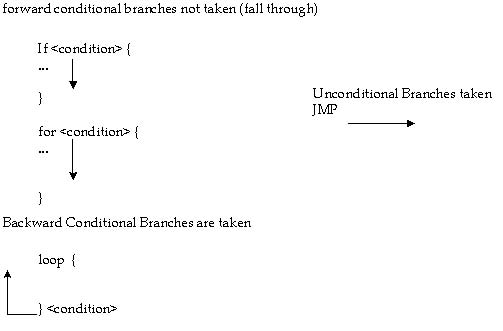
The Branch Target Buffer (BTB) stores the history of the previously seen branches and their targets. When a branch is prefetched, the BTB feeds the target address directly into the Instruction Fetch Unit (IFU). Once the branch is executed, the BTB is updated with the target address. Using the branch target buffer, branches that have been seen previously are dynamically predicted. The branch target buffer prediction algorithm includes pattern matching and up to four prediction history bits per target address. For example, a loop which is four iterations long should have close to 100% correct prediction. Adhering to the following guideline will improve branch prediction performance:
Program conditional branches (except for loops) so that the most executed branch immediately follows the branch instruction (that is, fall through).
Additionally, processors with MMX technology have a Return Stack Buffer (RSB), which can correctly predict return addresses for procedures that are called from different locations in succession. This increases further the benefit of unrolling loops which contain function calls, and removes the need to in-line certain procedures.
On the Pentium processor with MMX technology, branches may be mispredicted when the last byte of two branch instructions occur in the same aligned four byte section of memory, as shown in the figure below.
This may occur when there are two consecutive branches with no intervening instructions and the second instruction is only two bytes long (such as a jump relative +/- 128).
To avoid a misprediction in these cases, make the second branch longer by using a 16-bit relative displacement on the branch instruction instead of an 8-bit relative displacement.
Processors with MMX technology have four write buffers (versus two in Pentium processors without MMX technology). Additionally, the write buffers can be used by either the U-pipe or the V-pipe (versus one corresponding to each pipe in Pentium processors without MMX technology). Performance of critical loops can be improved by scheduling the writes to memory; when you expect to see write misses, you should schedule the write instructions in groups no larger than four, then schedule other instructions before scheduling further write instructions.
GUIDELINES FOR DEVELOPING MMX™ CODE
The following guidelines will help you develop fast and efficient MMX code that scales well across all processors with MMX technology.
The following section provides a list of rules and suggestions.
This section covers general optimization techniques that are important for the Intel Architecture.
On the Pentium processor, when a register is used as the base component, an additional clock cycle is used if that register is the destination of the immediately preceding instruction (assuming all instructions are already in the prefetch queue). For example:
add esi, eax ; esi is destination register
mov eax, [esi] ; esi is base, 1 clock penalty
Since the Pentium processor has two integer pipelines, a register used as the base or index component of an effective address calculation (in either pipe) causes an additional clock cycle if that register is the destination of either instruction from the immediately preceding clock cycle. This effect is known as Address Generation Interlock or AGI. To avoid the AGI, the instructions should be separated by at least one cycle by placing other instructions between them. The new MMX registers cannot be used as base or index registers, so the AGI does not apply for MMX register destinations.
Dynamic execution (P6-family) processors incur no penalty for the AGI condition.
Note that some instructions have implicit reads/writes to registers. Instructions that generate addresses implicitly through ESP (PUSH, POP, RET, CALL) also suffer from the AGI penalty. Examples follow:
sub esp, 24
; 1 clock cycle stall
push ebx
mov esp, ebp
;1 clock cycle stall
pop ebp
PUSH and POP also implicitly write to esp. This, however, does not cause an AGI when the next instruction addresses through ESP. Pentium processors "rename" ESP from PUSH and POP instructions to avoid the AGI penalty. An example follows:
push edi ; no stall
mov ebx, [esp]
On Pentium processors with MMX technology, instructions which include both an immediate and displacement fields are pairable in the U-pipe. When it is necessary to use constants, it is usually more efficient to use immediate data instead of loading the constant into a register first. If the same immediate data is used more than once, however, it is faster to load the constant in a register and then use the register multiple times. Following is an example:
mov result, 555 ; 555 is immediate, result is
; displacement
mov word ptr [esp+4], 1 ; 1 is immediate,4 is displacement
Since MMX instructions have two-byte opcodes (0x0F opcode map), any MMX instruction which uses base or index addressing with a 4-byte displacement to access memory will have a length of eight bytes. Instructions over seven bytes can limit decoding and should be avoided where possible (see Section 3.4.2). It is often possible to reduce the size of such instructions by adding the immediate value to the value in the base or index register, thus removing the immediate field.
The Intel486TM processor has a one clock penalty when using a full register immediately after a partial register was written. The Pentium processor is neutral in this respect. This is called a partial stall condition. The following example relates to the Pentium processor.
mov al, 0 ; 1
mov [ebp], eax ; 2 - No delay on the Pentium processor
The following example relates to the Intel486 processor.
mov al, 0 ; 1
; 2 1 clock penalty
mov [ebp], eax ; 3
Dynamic execution (P6-family) processors exhibit the same type of stall as the Intel486 processors, except that the cost is much higher. The read is stalled until the partial write retires, which can be considerably longer than one clock cycle.
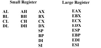
For best performance, avoid using a large register (for example, EAX) after writing a partial register (for example, AL, AH, AX) which is contained in the large register. This guideline will prevent partial stall conditions on dynamic execution processors and applies to all of the small and large register pairs:
AL AH AX EAX
BL BH BX EBX
CL CH CX ECX
DL DH DX EDX
SP ESP
EP EBP
SI ESI
DI EDI
Additional information on partial register stalls is in Section 3.2.4.
This section provides information on aligning code and data for Pentium and dynamic execution (P6-family) processors.
3.2.2.1 Code
Pentium and dynamic execution (P6-family) processors have a cache line size of 32 bytes. Since the prefetch buffers fetch on 16-byte boundaries, code alignment has a direct impact on prefetch buffer efficiency.
For optimal performance across the Intel Architecture family, it is recommended that:
3.2.2.2 Data
A misaligned access in the data cache or on the bus costs at least three extra clock cycles on the Pentium processor. A misaligned access in the data cache, which crosses a cache line boundary, costs nine to twelve clock cycles on dynamic execution (P6-family) processors. Intel recommends that data be aligned on the following boundaries for the best execution performance on all processors:
3.2.2.2.1 2-Byte Data
A 2-byte object should be fully contained within an aligned 4-byte word (that is, its binary address should be xxxx00, xxxx01, xxxx10, but not xxxx11).
3.2.2.2.2 4-Byte Data
The alignment of a 4-byte object should be on a 4-byte boundary.
3.2.2.2.3 8-Byte Data
An 8-byte datum (64 bit, for example, double precision real data types, all MMX packed register values) should be aligned on an 8-byte boundary.
On Pentium processors, a prefix on an instruction can delay the parsing and inhibit pairing of instructions.
The following list highlights the effects of instruction prefixes on the FIFO:
The impact on performance exists only when the FIFO does not hold at least two entries. As long as the decoder (D1 stage) has two instructions to decode there is no penalty. The FIFO will quickly become empty if the instructions are pulled from the FIFO at the rate of two per clock cycle. So, if the instructions just before the prefixed instruction suffer from a performance loss (for example, no pairing, stalls due to cache misses, misalignments, etc.), then the performance penalty of the prefixed instruction may be masked.
On dynamic execution (P6-family) processors, instructions longer than seven bytes in length limit the number of instructions decoded in each cycle (see Section 2.1.2). Prefixes add one to two bytes to the length of an instruction, possibly limiting the decoder.
It is recommended that, whenever possible, prefixed instructions not be used or that they be scheduled behind instructions which themselves stall the pipe for some other reason.
See Section 3.3 for more information on pairing of prefixed instructions.
On dynamic execution (P6-family) processors, when a 32-bit register (for example, EAX) is read immediately after 16 or 18-bit register (for example, AL, AH, AX) is written, the read is stalled until the write retires (a minimum of seven clock cycles). Consider the example below. The first instruction moves the value 8 into the AX register. The following instruction accesses the large register EAX. This code sequence results in a partial register stall.
MOV AX, 8
ADD ECX, EAX
Partial Stall occurs on access of the EAX register
This applies to all of the 8- and 16-bit/32-bit register pairs:
Pentium processors do not exhibit this penalty.
Because P6-family processors can execute code out of order, the instructions need not be immediately adjacent for the stall to occur. The following example also contains a partial stall:
MOV AL, 8
MOV EDX, 0x40
MOV EDI, new_value
ADD EDX, EAX
Partial Stall Occurs on access of the EAX register
In addition, any micro-ops that follow the stalled micro-op will also wait until the clock cycle after the stalled micro-op continues through the pipe. In general, to avoid stalls, do not read a large (32-bit) register (EAX) after writing a small (16- or 18-bit) register (AL) which is contained in the large register.
Special cases of reading and writing small and large register pairs have been implemented in dynamic execution processors in order to simplify the blending of code across processor generations. The special cases include the XOR and SUB instructions as shown in the following examples:
xor eax, eax
movb al, mem8
use eax <------- no partial stall
xor eax, eax
movw ax, mem16
use eax <------- no partial stall
sub ax, ax
movb al, mem8
use ax <------- no partial stall
sub eax, eax
movb al, mem8
use ax <------- no partial stall
xor ah, ah
movb al, mem8
use ax <------- no partial stall
In general, when implementing this sequence, always zero the large register then write to the lower half of the register. The special cases have been implemented for XOR and SUB when using EAX, EBX, ECX, EDX, EBP, ESP, EDI, and ESI.
Branch optimizations are the most important optimizations for dynamic execution (P6-family) processors. These optimizations also benefit the Pentium processor.
3.2.5.1 Dynamic Branch Prediction
Three elements of dynamic branch prediction are important:
The first element suggests that branches should be followed by code that will be executed. Never follow a branch with data.
To avoid the delay of one clock for taken branches, simply insert additional work between branches that are expected to be taken. This delay restricts the minimum size of loops to two clock cycles. If you have a very small loop that takes less than two clock cycles, unroll it.
The branch predictor correctly predicts regular patterns of branches. For example, it correctly predicts a branch within a loop that is taken on every odd iteration, and not taken on every even iteration.
3.2.5.2 Static Prediction on Dynamic Execution (P6-Family) Processors
On dynamic execution processors, branches that do not have a history in the BTB are predicted using a static prediction algorithm. The static prediction algorithm follows:
The performance penalty for static prediction is six clocks. The penalty for NO prediction or an incorrect prediction is greater than twelve clocks. The following chart illustrates the static branch prediction algorithm:
The following examples illustrate the basic rules for the static prediction algorithm.
A.Begin: MOV EAX, mem32
AND EAX, EBX
IMUL EAX, EDX
SHLD EAX, 7
JC Begin
In this example, the backwards (JC Begin) branch is not in the BTB the first time through, therefore, the BTB will not issue a prediction. The static predictor, however, will predict the branch to be taken, so a misprediction will not occur.
B. MOV EAX, mem32
AND EAX, EBX
IMUL EAX, EDX
SHLD EAX, 7
JC Begin
MOV EAX, 0
Begin: Call Convert
The first branch instruction (JC Begin) in this code segment is a conditional forward branch. It is not in the BTB the first time through, but the static predictor will predict the branch to fall through.
The Call Convert instruction will not be predicted in the BTB the first time it is seen by the BTB, but the call will be predicted as taken by the static prediction algorithm. This is correct for an unconditional branch.
In these examples, the conditional branch has only two alternatives: taken and not taken. Indirect branches, such as switch statements, computed GOTOs or calls through pointers, can jump to an arbitrary number of locations. If the branch has a skewed target destination (that is, 90% of the time it branches to the same address), then the BTB will predict accurately most of the time. If, however, the target destination is not predictable, performance can degrade quickly. Performance can be improved by changing the indirect branches to conditional branches that can be predicted.
Scheduling or pairing should be done in a way that optimizes performance across all processor generations. The following is a list of pairing and scheduling rules that can improve the speed of your code on Pentium and P6-family processors. In some cases, there are tradeoffs involved in reaching optimal performance on a specific processor; these tradeoffs vary based on the specific characteristics of the application. On superscalar Pentium processors, the order of instructions is very important to achieving maximum performance.
Reordering instructions increases the possibility of issuing two instructions simultaneously. Instructions that have data dependencies should be separated by at least one other instruction.
This section describes the rules you need to follow to pair MMX instructions with integer instructions. For each of the conditions listed in the following table, the subsection lists the rules that apply.
Several types of rules must be observed to allow pairing:
Note
Floating-point instructions are not pairable with MMX instructions.
For general pairing rules on Pentium processors, Optimizations for Intel's 32-bit Processors, Application Note AP-526, (Order Number 242816). The Pentium processors with MMX technology has relaxed some of the general pairing rules:
Pairing cannot be performed when the following two conditions occur:
|
Integer Instruction Pairable in U-Pipe |
Integer Instruction Pairable in V-Pipe |
||||
|
mov r, r |
alu r, i |
push r |
mov r, r |
alu r, i |
push r |
|
mov r, m |
alu m, i |
push i |
mov r, m |
alu m, i |
push I |
|
mov m, r |
alu eax, i |
pop r |
mov m, r |
alu eax, i |
pop r |
|
mov r, i |
alu m, r |
nop |
mov r, i |
alu m, r |
jmp near |
|
mov m, i |
alu r, m |
shift/rot by 1 |
mov m, i |
alu r, m |
jcc near |
|
mov eax, m |
inc/dec r |
shift by imm |
mov eax, m |
inc/dec r |
0F jcc |
|
mov m, eax |
inc/dec m |
test reg, r/m |
mov m, eax |
inc/dec m |
call near |
|
alu r, r |
lea r, m |
test acc, imm |
alu r, r |
lea r, m |
nop |
|
|
|
|
|
test reg, r/m |
test acc, imm |
3.3.2.1 Instructions that Cannot be Paired (NP)
Also see Section 3.3.2.2, No Pairing Allowed because of Register Dependencies.
3.3.2.2 Pairable Instructions Issued to U or V-pipes (UV)
3.3.2.3 Pairable Instructions Issued to U-pipe (PU)
3.3.2.4 Pairable Instructions Issued to V-pipe (PV)
These instructions can execute in either the U-pipe or the V-pipe but they are only paired when they are in the V-pipe. Since these instructions change the instruction pointer (eip), they cannot pair in the U-pipe since the next instruction may not be adjacent. Even when a branch in the U-pipe is predicted "not taken", the current instruction will not pair with the following instruction.
3.3.2.5 No Pairing Allowed Because of Register Dependencies
Instruction pairing is also affected by instruction operands. The following combinations cannot be paired because of register contention. Exceptions to these rules are given in the next section.
This limitation does not apply to a pair of instructions which write to the EFLAGS register (for example, two ALU operations that change the condition codes). The condition code after the paired instructions execute will have the condition from the V-pipe instruction.
Note that two instructions in which the first reads a register and the second writes to a condition knowing it (anti-dependence) may be paired. See following example:
mov eax, ebx
mov ebx, [ebp]
For purposes of determining register contention, a reference to a byte or word register is treated as a reference to the entire 32-bit register. Therefore,
mov al, 1
mov ah, 0
do not pair due to output dependencies on the contents of the EAX register.
3.3.2.6 Special Pairs
There are some special instructions that can be paired in spite of our "general" rule above. These special pairs overcome register dependencies and most involve implicit reads/writes to the esp register or implicit writes to the condition codes.
Stack Pointer:
Condition Codes:
Note that special pairs that consist of PUSH/POP instructions may have only immediate or register operands, not memory operands.
3.3.2.7 Restrictions On Pair Execution
There are some pairs that may be issued simultaneously but will not execute in parallel. The following two rules must be followed to pair an MMX instruction in the U-pipe and an integer instruction in the V-pipe.
The instructions above add the contents of the register and the value at the memory location, then put the result in the register. An add with a memory operand takes two clocks to execute. The first clock loads the value from cache and the second clock performs the addition. Since there is only one memory access in the U-pipe instruction, the add in the V-pipe can start in the same cycle.
add meml, eax ; 1
(add) ; 2
(add) add mem2, ebx ; 3
(add) ; 4
(add) ; 5
The above instructions add the contents of the register to the memory location and store the result at the memory location. An add with a memory result takes three clocks to execute. The first clock loads the value, the second performs the addition and the third stores the result. When paired, the last cycle of the U-pipe instruction overlaps with the first cycle of the V-pipe instruction execution.
No other instructions may begin execution until the instructions already executing have completed.
To best expose opportunities for scheduling and pairing, it is better to issue a sequence of simple instructions rather than a complex instruction that takes the same number of cycles. The simple instruction sequence can take advantage of more issue slots. The load/store style code generation requires more registers and increases code size. To compensate for the extra registers needed, extra effort should be put into register allocation and instruction scheduling so that extra registers are used only when parallelism increases.
This section specifies guidelines for pairing MMX instructions with each other and with integer instructions.
3.3.3.1 Pairing Two MMXTM Instructions:
3.3.3.2 Pairing an Integer Instruction in the U-Pipe with an MMXTM Instruction in the V-Pipe
3.3.3.3 Pairing an MMXTM Instruction in the U-Pipe with an Integer Instruction in the V-Pipe
3.3.3.4 Scheduling Rules
All MMX instructions may be pipelined including the multiply instructions. All instructions take a single clock to execute except MMX multiply instructions which take three clocks.
Since multiply instructions take three clocks to execute, the result of a multiply instruction can be used only by other instructions issued three clocks later. For this reason, avoid scheduling a dependent instruction in the two instruction pairs following the multiply.
As mentioned in Section 2.1.1, the store of a register after writing the register must wait for two clocks after the update of the register. Scheduling the store two clock cycles after the update avoids a pipeline stall.
The following section describes instruction selection optimizations.
An MMX instruction may have two register operands ("OP reg, reg") or one register and one memory operand ("OP reg, mem"), where OP represents the instruction operand and, reg represents the register and mem represents memory. "OP reg, mem" instructions are useful, in some cases, to reduce register pressure, increase the number of operations per cycle, and reduce code size.
The following discussion assumes that the memory operand is present in the data cache. If it is not, then the resulting penalty is usually large enough to obviate the scheduling effects discussed in this section.
In Pentium processors, "OP reg, mem" MMX instructions do not have longer latency than "OP reg, reg" instructions (assuming a cache hit). They do have more limited pairing opportunities, however (see Section 3.3.1). In dynamic execution (P6-family) processors, "OP reg, mem" MMX instructions translate into two micro-ops (as opposed to one uop for the "OP reg, reg" instructions). Thus, they tend to limit decoding bandwidth (see Section 2.1.2) and occupy more resources than "OP reg, reg" instructions.
Recommended usage of "OP reg, mem" instructions depends on whether the MMX code is memory-bound (that is, execution speed is limited by memory accesses). As a rule of thumb, an MMX code section is considered to be memory-bound if the following inequality holds:
![]()
For memory-bound MMX code, Intel recommends to merge loads whenever the same memory address is used more than once. This reduces the number of memory accesses.
Example:
OP MM0, [address A]
OP MM1, [address A]
becomes:
MOVQ MM2, [address A]
OP MM0, MM2
OP MM1, MM2
For MMX code that is not memory-bound, load merging is recommended only if the same memory address is used more than twice. Where load merging is not possible, usage of "OP reg, mem" instructions is recommended to minimize instruction count and code size.
Example:
MOVQ MM0, [address A]
OP MM1, MM0
becomes:
OP MM1, [address A]
In many cases, a "MOVQ reg, reg" and "OP reg, mem" can be replaced by a "MOVQ reg, mem" and "OP reg, reg". This should be done where possible, since it saves one uop on dynamic execution processors.
Example: (here OP is a symmetric operation)
MOVQ MM1, MM0 (1 micro-op)
OP MM1, [address A] (2 micro-ops)
becomes:
MOVQ MM1, [address A] (1 micro-op)
OP MM1, MM0 (1 micro-op)
On Pentium processors, instructions greater than seven bytes in length cannot be executed in the V-pipe. In addition, two instructions cannot be pushed into the instruction FIFO (see Section 2.1.1) unless both are seven bytes or less in length. If only one instruction is pushed into the FIFO, pairing will not occur unless the FIFO already contains at least one instruction. In code where pairing is very high (this often happens in MMX code) or after a mispredicted branch, the FIFO may be empty, leading to a loss of pairing whenever the instruction length is over seven bytes.
In addition, dynamic execution (P6-family) processors can only decode one instruction at a time when an instruction is longer than seven bytes.
So, for best performance on all Intel processors, use simple instructions that are less than eight bytes in length (see Section 3.4.1 for one way to reduce instruction size).
Cache behavior can dramatically affect the performance of your application. By having a good understanding of how the cache works, you can structure your code to take best advantage of cache capabilities. For more information on the structure of the cache, see Section 2.2.
When a data access to a cacheable address misses the data cache, the entire cache line is brought into the cache from external memory. This is called a line fill. On Pentium and dynamic execution (P6-family) processors, these data arrive in a burst composed of four 8-byte sections in the following burst order:
|
1st Address |
2nd Address |
3rd Address |
4th Address |
|
0h |
8h |
10h |
18h |
|
8h |
0h |
18h |
10h |
|
10h |
18h |
0h |
8h |
|
18h |
10h |
8h |
0h |
Data are available for use in the order that they arrive from memory. If an array of data is being read serially, it is preferable to access it in sequential order so that each data item will be used as it arrives from memory.
Arrays with a size which is a multiple of 32 bytes should start at the beginning of a cache line. By aligning on a 32-byte boundary, you take advantage of the line fill ordering and match the cache line size. Arrays with sizes which are not multiples of 32 bytes should begin at 32- or 16-byte boundaries (the beginning or middle of a cache line). In order to align on a 16-or 32- byte boundary, you may need to pad the data. If this is necessary, try to locate data (variables or constants) in the padded space.
Dynamic execution (P6-family) processors have a "write allocate by read-for-ownership" cache, whereas the Pentium processor has a "no-write-allocate; write through on write miss" cache.
On dynamic execution (P6-family) processors, when a write occurs and the write misses the cache, the entire 32-byte cache line is fetched. On the Pentium processor, when the same write miss occurs, the write is simply sent out to memory.
Write allocate is generally advantageous, since sequential stores are merged into burst writes, and the data remains in the cache for use by later loads. This is why dynamic execution (P6-family) processors adopted this write strategy, and why some Pentium processor system designs implement it for the L2 cache, even though the Pentium processor uses write-through on a write miss.
Write allocate can be a disadvantage in code where:
When a large number of writes occur within an application, as in the example program below, and both the stride is longer than the 32-byte cache line and the array is large, every store on a dynamic execution (P6-family) processor will cause an entire cache line to be fetched. In addition, this fetch will probably replace one (sometimes two) dirty cache line.
The result is that every store causes an additional cache line fetch and slows down the execution of the program. When many writes occur in a program, the performance decrease can be significant. The Sieve of Erastothenes program is a simplistic example that demonstrates these cache effects. In this example, a large array is stepped through in increasing strides while writing a single value of the array with zero.
Note:
This is a very simplistic example used only to demonstrate cache effects; many other optimizations are possible in this code.
Sieve of Erastothenes example:
boolean array[2..max]
for(i=2;i<max;i++) {
array := 1;
}
for(i=2;i<max;i++) {
if( array[i] ) {
for(j=2;j<max;j+=i) {
array[j] := 0; /*here we assign memory to 0 causing
fetch within the j loop */
}
}
}
Two optimizations are available for this specific example. One is to pack the array into bits, thereby reducing the size of the array, which in turn reduces the number of cache line fetches. The second is to check the value prior to writing, thereby reducing the number of writes to memory (dirty cache lines).
In the program above, 'Boolean' is a char array. It may well be better, in some programs, to make the "boolean" array into an array of bits, packed so that read-modify-writes are done (since the cache protocol makes every read into a read-modify-write). But, in this example, the vast majority of strides are greater than 256 bits (one cache line of bits), so the performance increase is not significant.
Another optimization is to check if the value is already zero before writing.
boolean array[2..max]
for(i=2;i<max;i++) {
array := 1;
}
for(i=2;i<max;i++) {
if( array[i] ) {
for(j=2;j<max;j+=i) {
if( array[j] != 0 ) { /* check to see if value is
array[j] := 0;
}
}
}
}
The external bus activity is reduced by half because most of the time in the Sieve program the data is already zero. By checking first, you need only one burst bus cycle for the read and you save the burst bus cycle for every line you do not write. The actual write back of the modified line is no longer needed, therefore saving the extra cycles.
Note:
This operation benefits P6-family processors but may not enhance the performance of Pentium processors. As such, it should not be considered generic. Write allocate is generally a performance advantage in most systems, since sequential stores are merged into burst writes, and the data remain in the cache for use by later loads. This is why P6-family processors use this strategy, and why some Pentium processor-based systems implement it for the L2 cache.
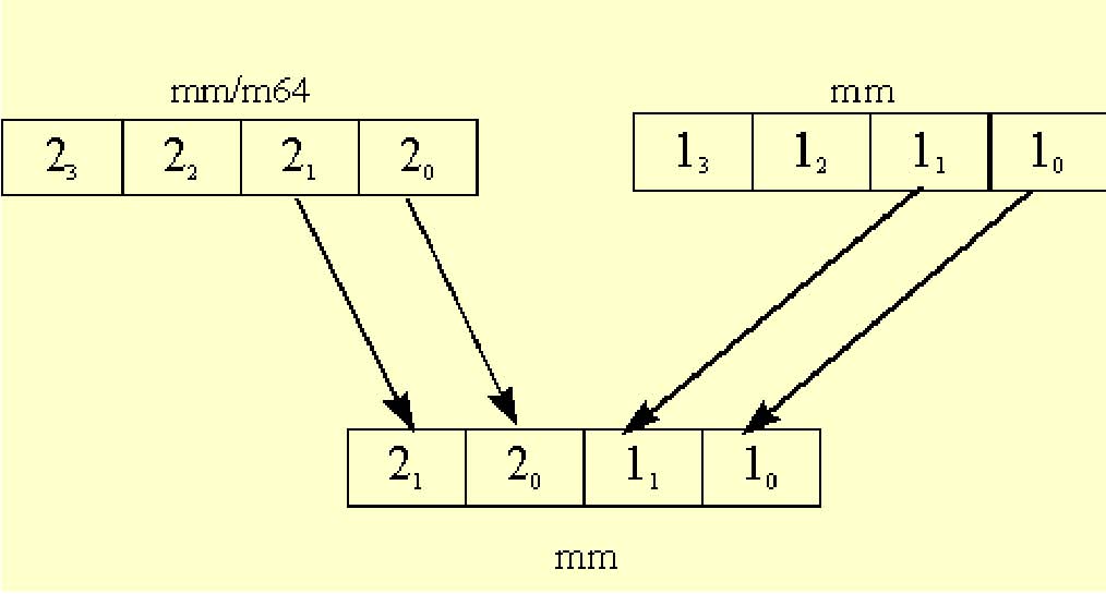
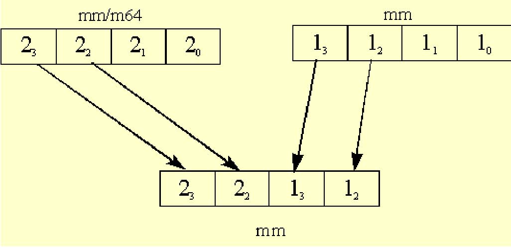
The MMX registers allow you to move large quantities of data without stalling the processor. Instead of loading single array values that are 8-, 16-, or 32-bits long, consider loading the values in a single quadword, then incrementing the structure or array pointer accordingly.
Any data that will be manipulated by MMX instructions should be loaded using either;
All SIMD data should be stored using the MMX instruction that stores a 64-bit operand (for example, MOVQ m64, MM0).
The goal of these recommendations is twofold: First, the loading and storing of SIMD data is more efficient using the larger quadword data block sizes. Second, this helps to avoid the mixing of 8-, 16-, or 32-bit load and store operations with 64-bit MMX load and store operations to the same SIMD data. This, in turn, prevents situations in which a) small loads follow large stores to the same area of memory, or b) large loads follow small stores to the same area of memory. Dynamic execution processors will stall in these situations. (See list of rules in Section 3.1.1.).
Consider the following examples. In the first case, there is a large load after a series of small stores to the same area of memory (beginning at memory address "mem"). The large load will stall in this case:
MOV mem, eax ; store dword to address "mem"
MOV mem + 4, ebx ; store dword to address "mem + 4"
:
:
MOVQ mm0, mem ; load qword at address "mem", stalls
The MOVQ must wait for the stores to write memory before it can access all the data it requires. This stall can also occur with other data types (for example, when bytes or words are stored and then words or doublewords are read from the same area of memory). When you change the code sequence as follows, the processor can access the data without delay:
MOVD mm1, ebx ; build data into a qword first before
; storing it to memory
MOVD mm2, eax
PSLLQ mm1, 32
POR mm1, mm2
MOVQ mem, mm1 ; store SIMD variable to "mem" as a
; qword
:
:
MOVQ mm0, mem ; load qword SIMD variable "mem",no
;stall
In the second case, there is a series of small loads after a large store to the same area of memory (beginning at memory address "mem"). The small loads will stall in this case:
MOVQ mem, mm0 ; store qword to address
; "mem"
:
:
MOV bx, mem + 2 ; load word at address
; "mem + 2", stalls
MOV cx, mem + 4 ; load word at address
; "mem + 4", stalls
The word loads must wait for the quadword store to write to memory before they can access the data they require. This stall can also occur with other data types (for example, when doublewords or words are stored and then words or bytes are read from the same area of memory). When you change the code sequence as follows, the processor can access the data without delay:
MOVQ mem, mm0 ; store qword to address "mem"
:
:
MOVQ mm1, mem ; load qword at address "mem"
MOVD eax, mm1 ; transfer "mem + 2" to ax from
; MMX register not memory
PSRLQ mm1, 32
SHR eax, 16
MOVD ebx, mm1 ; transfer "mem + 4" to bx from
; MMX register, not memory
AND ebx, 0ffffh
These transformations, in general, increase the number the instructions required to perform the desired operation. For dynamic execution (P6-family) processors, the performance penalty due to the increased number of instructions is more than offset by the benefit. For Pentium processors, however, the increased number of instructions can negatively impact performance, since they do not benefit from the code transformations above. For this reason, careful and efficient coding of these transformations is necessary to minimize any potential negative impact to Pentium processor performance.
It is beneficial to understand how memory is accessed and filled. A memory-to-memory fill (for example a memory-to-video fill) is defined as a 32-byte (cache line) load from memory which is immediately stored back to memory (such as a video frame buffer). The following are guidelines for obtaining higher bandwidth and shorter latencies for sequential memory fills (video fills). These recommendations are relevant for all Intel Architecture processors with MMX technology and refer to cases in which the loads and stores do not hit in the second level cache.
3.6.2.1 Memory Fills
3.6.2.1.1 Increasing Memory Bandwidth Using the MOVQ Instruction
Loading any value will cause an entire cache line to be loaded into the on-chip cache. But, using MOVQ to store the data back to memory instead of using 32-bit stores (for example, MOVD) will reduce by half the number of stores per memory fill cycle. As a result, the bandwidth of the memory fill cycle increases significantly. On some Pentium processor-based systems, 30% higher bandwidth was measured when 64-bit stores were used instead of 32-bit stores. Additionally, on dynamic execution processors, this avoids a partial memory access when both the loads and stores are done with the MOVQ instruction.
3.6.2.1.2 Increasing Memory Bandwidth by Loading and Storing To and From the Same DRAM Page
DRAM is divided into pages (which are not the same as Operating System (OS) pages. The size of a DRAM page is a function of the DRAM's size and organization. Page sizes of several Kbytes are common. Like OS pages, DRAM pages are constructed of sequential addresses. Sequential memory accesses to the same DRAM page have shorter latencies than sequential accesses to different DRAM pages. In many systems the latency for a page miss (that is, an access to a different page instead of the page previously accessed) can be twice as large as the latency of a memory page hit (access to the same page as the previous access). Therefore, if the loads and stores of the memory fill cycle are to the same DRAM page, we can see a significant increase in the bandwidth of the memory fill cycles.
3.6.2.1.3 Increasing the Memory Fill Bandwidth by Using Aligned Stores
Unaligned stores will double the number of stores to memory. Intel strongly recommends that quadword stores be 8-byte aligned. Four aligned quadword stores are required to write a cache line to memory. If the quadword store is not 8-byte aligned, then two 32 bit writes result from each MOVQ store instruction. On some systems, a 20% lower bandwidth was measured when 64 bit misaligned stores were used instead of aligned stores.
3.6.2.2 Video Fills
3.6.2.2.1 Use 64 Bit Stores to Increase the Bandwidth to Videob
Although the PCI bus between the processor and the Frame buffer is 32 bits wide, using MOVQ to store to video is faster on most Pentium processor-based systems than using twice as many 32-bit stores to video. This occurs because the bandwidth to PCI write buffers (which are located between the CPU and PCI bus) is higher when quadword stores are used.
3.6.2.2.2 Increase the Bandwidth to Video Using Aligned Stores
When a non-aligned store is encountered, there is a dramatic decrease in the bandwidth to video. Misalignment causes twice as many stores, and, in addition, the latency of stores on the PCI bus (to the Frame buffer) is much longer. On the PCI bus, it is not possible to burst sequential misaligned stores. On Pentium processor-based systems, a decrease of 80% in the video fill bandwidth is typical when misaligned stores are used instead of aligned stores.
MMX™ CODE DEVELOPMENT STRATEGY
In general, developing fast applications for Intel Architecture (IA) processors is not difficult. An understanding of the architecture and good development practices make the difference between a fast application and one that runs significantly slower than its full potential. Intel Architecture processors with MMXTM technology add a new dimension to code development. Performance increase can be significant, though the conversion techniques are straight forward. In order to develop MMX technology code, examine the current implementation and determine the best way to take advantage of MMX technology instructions. If you are starting a new implementation, design the application with MMX technology in mind from the start.
Whether adapting an existing application or creating a new one, using MMX technology instructions to optimal advantage requires consideration of several issues. Generally, you should look for code segments that are computationally intensive, that are adaptable to integer implementations, and that support efficient use of the cache architecture. Several tools are provided in the Intel Performance Tool Set to aid in this evaluation and tuning.
Several questions should be answered before beginning your implementation:
Step one: Determine which code to convert.
Most applications have sections of code that are highly compute-intensive. Examples include speech compression algorithms and filters, video display routines, and rendering routines. These routines are generally small, repetitive loops, operating on 8- or 16-bit integers, and take a sizable portion of the application processing time. It is these routines that will yield the greatest performance increase when converted to MMXTM technology optimized libraries code. Encapsulating these loops into MMX technology-optimized libraries will allow greater flexibility in supporting platforms with and without MMX technology.
A performance optimization tool such as Intel's VTune visual tuning tool may be used to isolate the compute-intensive sections of code. Once identified, an evaluation should be done to determine whether the current algorithm or a modified one will give the best performance. In some cases, it is possible to improve performance by changing the types of operations in the algorithm. Matching the algorithms to MMX technology instruction capabilities is key to extracting the best performance.
Step two: Determine whether the algorithm contains floating-point or integer data.
If the current algorithm is implemented with integer data, then simply identify the portions of the algorithm that use the most microprocessor clock cycles. Once identified, re-implement these sections of code using MMX technology instructions.
If the algorithm contains floating-point data, then determine why floating-point was used. Several reasons exist for using floating-point operations: performance, range and precision. If performance was the reason for implementing the algorithm in floating-point, then the algorithm is a candidate for conversion to MMX technology instructions to increase performance.
If range or precision was an issue when implementing the algorithm in floating point then further investigation needs to be made. Can the data values be converted to integer with the required range and precision? If not, this code is best left as floating-point code.
When generating MMX technology code, it is important to keep in mind that the eight MMX technology registers are aliased upon the floating-point registers. Switching from MMX technology instructions to floating-point instructions can take up to fifty clock cycles, so it is best to minimize switching between these instruction types. Do not intermix MMX technology code and floating-point code at the instruction level. If an application does perform frequent switches between floating-point and MMX technology instructions, then consider extending the period that the application stays in the MMX technology instruction stream or floating-point instruction stream to minimize the penalty of the switch.
When writing an application that uses both floating-point and MMX technology instructions, use the following guidelines for isolating instruction execution:
For example:
FP_code:
..
.. /* leave the floating-point stack empty
*/
MMX_code:
...
EMMS /* empty the MMX Technology registers */
FP_code1:
...
... /* leave the floating-point stack empty
*/
Additional information on the floating-point programming model can be found in the Pentium® Processor Family Developer's Manual: Volume 3, Architecture and Programming, (Order Number 241430).
Step three: Always call the EMMS instruction at the end of your MMX technology code.
Since the MMX technology registers are aliased on the floating-point registers, it is very important to clear the MMX technology registers before issuing a floating-point instruction. Use the EMMS instruction to clear the MMX technology registers and set the value of the floating-point tag word (TW) to empty (that is, all ones). This instruction should be inserted at the end of all MMX technology code segments to avoid an overflow exception in the floating-point stack when a floating-point instruction is executed.
Step four: Determine if MMX technology is available.
MMX technology can be included in your application in two ways: Using the first method, have the application check for MMX technology during installation. If MMX technology is available, the appropriate libraries can be installed. The second method is to check during program execution and install the proper libraries at runtime. This is effective for programs that may be executed over a network.
To determine whether you are executing on a processor with MMX technology, your application should check the Intel Architecture feature flags. The CPUID instruction returns the feature flags in the EDX register. Based on the results, the program can decide which version of code is appropriate for the system.
Existence of MMX technology support is denoted by bit 23 of the feature flags. When this bit is set to 1 the processor has MMX technology support. The following code segment loads the feature flags in EDX and tests the result for MMX technology. Additional information on CPUID usage may be found in Intel Processor Identification with CPUID Instruction, Application Note AP-485, (Order Number 241618).
… ; identify existence of CPUID instruction
… ;
… ; identify Intel Processor
… ;
mov EAX, 1 ; request for feature flags
CPUID ; 0Fh, 0A2h CPUID Instruction
test EDX, 00800000h ; is MMX technology Bit(bit 23)in feature
jnz Found
Step five: Make sure your data is aligned.
Many compilers allow you to specify the alignment of your variables using controls. In general this guarantees that your variables will be on the appropriate boundaries. However, if you discover that some of the variables are not appropriately aligned as specified, then align the variable using the following C algorithm. This aligns a 64-bit variable on a 64-bit boundary. Once aligned, every access to this variable will save three clock cycles.
if (NULL == (new_ptr = malloc(new_value +1)* sizeof (var_struct))
mem_tmp = new_ptr;
mem_tmp /= 8;
new_tmp_ptr = (var_struct*) ((Mem_tmp+1) * 8);
Another way to improve data alignment is to copy the data into locations that are aligned on 64-bit boundaries. When the data is accessed frequently this can provide a significant performance improvement.
As a matter of convention, compilers allocate anything that is not static on the stack and it may be convenient to make use of the 64-bit data quantities that are stored on the stack. When this is necessary, it is important to make sure the stack is aligned. The following code in the function prologue and epilogue will make sure the stack is aligned.
Prologue:
push ebp ; save old frame ptr
mov ebp, esp ; make new frame ptr
sub ebp, 4 ; make room of stack ptr
and ebp, 0FFFFFFFC ; align to 64 bits
mov [ebp],esp ; save old stack ptr
mov esp, ebp ; copy aligned ptr
sub esp, FRAMESIZE ; allocate space
… callee saves, etc
epilogue:
… callee restores, etc
mov esp, [ebp]
pop ebp
ret
In cases where misalignment is unavoidable for some frequently accessed data, it may be useful to copy the data to an aligned temporary storage location.
MMX technology uses an SIMD technique to exploit the inherent parallelism of many multimedia algorithms. To get the most performance out of MMX technology code, data should be formatted in memory according to the guidelines below.
Consider a simple example of adding a 16-bit bias to all the 16-bit elements of a vector. In regular scalar code, you would load the bias into a register at the beginning of the loop, access the vector elements in another register, and do the addition one element at a time.
Converting this routine to MMX technology code, you would expect a four times speedup since MMX technology instructions can process four elements of the vector at a time using the MOVQ instruction, and perform four additions at a time using the PADDW instruction. However, to achieve the expected speedup, you would need four contiguous copies of the bias in the MMX technology register when doing the addition.
In the original scalar code, only one copy of the bias was in memory. To use MMX technology instructions, you could use various manipulations to get four copies of the bias in an MMX technology register. Or, you could format your memory in advance to hold four contiguous copies of the bias. Then, you need only load these copies using one MOVQ instruction before the loop, and the four times speedup is achieved. For another interesting example of this type of data arrangement see Section 5.6.
The new 64-bit packed data types defined by MMX technology creates more potential for misaligned data accesses. The data access patterns of many algorithms are inherently misaligned when using MMX technology instructions and other packed data types. A simple example of this is an FIR filter. An FIR filter is effectively a vector dot product in the length of the number of coefficient taps. If the filter operation of data element i is the vector dot product that begins at data element j (data [ j ] *coeff [0] + data [j+1]*coeff [1]+...+data [j+num_of_taps-1]*coeff [num_of_taps-1] ), then the filter operation of data element i+1 begins at data element j+1.
Section 4.6 covers aligning 64-bit data in memory. Assuming you have a 64-bit aligned data vector and a 64-bit aligned coefficients vector, the filter operation on the first data element will be fully aligned. For the filter operation on the second data element, however, each access to the data vector will be misaligned! Duplication and padding of data structures may be used to avoid the problem of data accesses in algorithms which are inherently misaligned. Using MMXTM Technology Instructions to Compute a 16-Bit Real FIR Filter, Application Note #559, (Order Number 243044) shows an example of how to avoid the misalignment problem in the FIR filter.
Note that the duplication and padding technique overcomes the misalignment problem, thus avoiding the expensive penalty for misaligned data access, at the price of increasing the data size. When developing your code, you should consider this tradeoff and use the option which gives the best performance.
The best way to tune your application once it is functioning correctly is to use a profiler that measures the application while it is running on a system. Intel's VTune visual tuning tool is such a tool and can help you to determine where to make changes in your application to improve performance. Additionally, Intel's processors provide performance counters on-chip. Section 6.1 documents these counters and provides an explanation of how to use them.
MMX™ CODING TECHNIQUES
This section contains several simple examples that will help you to get started in coding your application. The goal is to provide simple, low-level operations that are frequently used. Each example uses the minimum number of instructions necessary to achieve best performance on Pentium(R) and P6-family processors.
These examples do not address scheduling as we assume you will incorporate the examples in longer code sequences.
The MMXTM technology provides several instructions that are used to pack and unpack data in the MMX technology registers. The unpack instructions can be used to zero-extend an unsigned number. The following example assumes the source is a packed-word (16-bit) data type.
Input: MM0 : Source value;
MM7 : 0
A local variable can be used instead of the register MM7, if desired.
Output: MM0 : two zero-extended 32-bit doublewords from 2 LOW end words
MM1 : two zero-extended 32-bit doubleword from 2 HIGH end words
MOVQ MM1, MM0 ; copy source
PUNPCKLWD MM0, MM7 ; unpack the 2 low end words
; into two 32-bit double word
PUNPCKHWD MM1, MM7 ; unpack the 2 high end words into two
; 32-bit double word
Signed numbers should be sign-extended when unpacking the values. This is done differently than the zero-extend shown above. The following example assumes the source is a packed-word (16-bit) data type.
Input: MM0 : source value
Output: MM0 : two sign-extended 32-bit doublewords from the two LOW end words
MM1 : two sign-extended 32-bit doublewords from the two HIGH end words
PUNPCKHWD MM1, MM0 ; unpack the 2 high end words of the
; source into the second and fourth
; words of the destination
PUNPCKLWD MM0, MM0 ; unpack the 2 low end words of the
; source into the second and fourth
; words of the destination
PSRAD MM0, 16 ; Sign-extend the 2 low end words of
; the source into two 32-bit signed
; doublewords
PSRAD MM1, 16 ; Sign-extend the 2 high end words of
; the source into two 32-bit signed
;doublewords
The PACK instructions pack two values into the destination register in a predetermined order. Specifically, the PACKSSDW instruction packs two signed doublewords from the source operand and two signed doublewords from the destination operand into four signed words in the destination register as shown in the figure below.
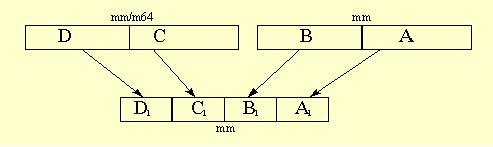
The following example interleaves the two values in the destination register, as shown in the figure below.
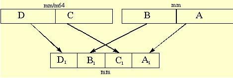
This example uses signed doublewords as source operands and the result is interleaved signed words. The pack instructions can be performed with or without saturation as needed.
Input: MM0 : Signed source1 value
MM1 : Signed source2 value
Output: MM0 : The first and third words contain the signed-saturated doublewords from MM0
MM0. The second and fourth words contain the signed-saturated doublewords from MM1
PACKSSDW MM0, MM0 ; pack and sign saturate
PACKSSDW MM1, MM1 ; pack and sign saturate
PUNPKLWD MM0, MM1 ; interleave the low end 16-bit values of the
; operands
The pack instructions always assume the source operands are signed numbers. The result in the destination register is always defined by the pack instruction that performs the operation. For example, the PACKSSDW instruction, packs each of the two signed 32-bit values of the two sources into four saturated 16-bit signed values in the destination register. The PACKUSWB instruction, on the other hand, packs each of the four signed 16-bit values of the two sources into four saturated 8-bit unsigned values in the destination. A complete specification of the MMX technology instruction set can be found in the Intel Architecture MMX TM Technology Programmers Reference Manual, (Order Number 243007).
This example is similar to the last except that the resulting words are not saturated. In addition, in order to protect against overflow, only the low order 16-bits of each doubleword are used in this operation.
Input: MM0 : signed source value
MM1 : signed source value
Output: MM0 : The first and third words contain the low 16-bits of the doublewords in MM0 : The second and fourth words contain the low 16-bits of the doublewords in MM1 PSLLD MM1, 16 ; shift the 16 LSB from each of the double ; words values to the 16 MSB position PAND MM0, {0,ffff,0,ffff} ; mask to zero the 16 MSB of each ; doubleword value POR MM0, MM1 ; merge the two operands
The unpack instructions perform an interleave merge of the data elements of the destination and source operands into the destination register. The following example merges the two operands into the destination registers without interleaving. For example, take two adjacent elements of a packed-word data type in source1; place this value in the low 32-bits of the results. Then take two adjacent elements of a packed-word data type in source2; place this value in the high 32-bits of the results. One of the destination registers will have the combination shown in Figure 5-3.
The other destination register will contain the opposite combination as in Figure 5-4.
The following example unpacks two packed-word sources in a non-interleaved way. The trick is to use the instruction which unpacks doublewords to a quadword, instead of using the instruction which unpacks words to doublewords.
Input: MM0 : packed-word source value
MM1 : packed-word source value
Output: MM0 : contains the two low end words of the original sources, non-interleaved
MM2 : contains the two high end words of the original sources, non-interleaved.
MOVQ MM2, MM0 ; copy source1
PUNPCKLDQ MM0, MM1 ; replace the two high end words of MM0
; with the two low end words of MM1
; leave the two low end words of MM0
; in place
PUNPCKHDQ MM2, MM1 ; move the two high end words of MM2 to the
; two low end words of MM2; place the two
; high end words of MM1 in the two high end
; words of MM2
Complex multiplication is an operation which requires four multiplications and two additions. This is exactly how the PMADDWD instruction operates. In order to use this instruction you need only to format the data into four 16-bit values. The real and imaginary components should be 16-bits each.
Let the input data be Dr and Di where Dr = real component of the data Di = imaginary component of the data
Format the constant complex coefficients in memory as four 16-bit values [Cr -Ci Ci Cr]. Remember to load the values into the MMX technology register using a MOVQ instruction.
Input: MM0 : a complex number Dr, Di
MM1 : constant complex coefficient in the form[Cr-Ci Ci Cr]
Output: MM0 : two 32-bit dwords containing [ Pr Pi ]
The real component of the complex product is Pr = Dr*Cr - Di*Ci, and the imaginary component of the complex product is
Pi = Dr*Ci + Di*Cr
PUNPCKLDQ MM0,MM0 ; This makes [Dr Di Dr Di]
PMADDWD MM0, MM1 ; and you're done, the result is
; [(Dr*Cr-Di*Ci)(Dr*Ci+Di*Cr)]
Note that the output is a packed word. If needed, a pack instruction can be used to convert the result to 16-bit (thereby matching the format of the input).
This example computes the absolute difference of two unsigned numbers. It assumes an unsigned packed-byte data type. Here, we make use of the subtract instruction with unsigned saturation. This instruction receives UNSIGNED operands and subtracts them with UNSIGNED saturation. This support exists only for packed bytes and packed words, NOT for packed dwords.
Input: MM0: source operand
MM1: source operand
Output: MM0: The absolute difference of the unsigned operands
MOVQ MM2, MM0 ; make a copy of MM0
PSUBUSB MM0, MM1 ; compute difference one way
PSUBUSB MM1, MM2 ; compute difference the other way
POR MM0, MM1 ; OR them together
This example will not work if the operands are signed. See the next example for signed absolute differences.
This example computes the absolute difference of two signed numbers. There is no MMX technology instruction subtract which receives SIGNED operands and subtracts them with UNSIGNED saturation. The technique used here is to first sort the corresponding elements of the input operands into packed-words of the maxima values, and packed-words of the minima values. Then the minima values are subtracted from the maxima values to generate the required absolute difference. The key is a fast sorting technique which uses the fact that B= XOR(A, XOR(A,B)) and A = XOR(A,0). Thus in a packed data type, having some elements being XOR(A,B) and some being 0, you could XOR such an operand with A and receive in some places values of A and in some values of B. The following examples assume a packed-word data type, each element being a signed value.
Input: MM0: signed source operand
MM1: signed source operand
Output: MM0: The absolute difference of the signed operands
MOVQ MM2, MM0 ; make a copy of source1 (A)
PCMPGTW MM0, MM1 ; create mask of source1>source2 (A>B)
MOVQ MM4, MM2 ; make another copy of A
PXOR MM2, MM1 ; Create the intermediate value of the swap
; operation - XOR(A,B)
PAND MM2, MM0 ; create a mask of 0s and XOR(A,B)
; elements. Where A>B there will be a value
; XOR(A,B) and where A<=B there will be 0.
MOVQ MM3, MM2 ; make a copy of the swap mask
PXOR MM4, MM2 ; This is the minima - XOR(A, swap mask)
PXOR MM1, MM3 ; This is the maxima - XOR(B, swap mask)
PSUBW MM1, MM4 ; absolute difference = maxima-minima
To compute |x|, where x is signed. This example assumes signed words to be the operands.
Input: MM0 : signed source operand
Output: MM1 : ABS(MM0)
MOVQ MM1, MM0 ; make a copy of x
PSRAW MM0,15 ; replicate sign bit (use 31 if doing
; DWORDS)
PXOR MM0, MM1 ; take 1's complement of just the
; negative fields
PSUBS MM1, MM0 ; add 1 to just the negative fields
Note that the absolute value of the most negative number (that is, 8000 hex for 16-bit) does not fit, but this code does something reasonable for this case; it gives 7fff which is off by one.
This example shows how to clip a signed value to the signed range [HIGH, LOW]. Specifically, if the value is less than LOW or greater than HIGH then clip to LOW or HIGH, respectively. This technique uses the packed-add and packed-subtract instructions with unsigned saturation, which means that this technique can only be used on packed-bytes and packed-words data types.
The following example uses the constants packed_max and packed_min.
The following examples shows the operation on word values. For simplicity we use the following constants (corresponding constants are used in case the operation is done on byte values):
The examples illustrate the operation on word values.
Input: MM0 : Signed source operands
Output: MM0 : Signed operands clipped to the unsigned range [HIGH, LOW]
PADD MM0, PACKED_MIN ; add with no
; saturation 0x8000
; to convert to
; unsigned
PADDUSW MM0, (PACKED_USMAX - HIGH_US) ; in effect this clips
; to HIGH
PSUBUSW MM0, (PACKED_USMAX - HIGH_US + LOW_US) ;
; in effect
; this clips to LOW
PADDW MM0, PACKED_LOW ; undo the previous two
; offsets
The code above converts values to unsigned numbers first and then clips them to an unsigned range. The last instruction converts the data back to signed data and places the data within the signed range. Conversion to unsigned data is required for correct results when the quantity (HIGH - LOW) < 0x8000.
IF (HIGH - LOW) >= 0x8000, the algorithm can be simplified to the following:
Input: MM0 : Signed source operands
Output: MM0 : Signed operands clipped to the unsigned range [HIGH, LOW]
PADDSSW MM0, (PACKED_MAX - PACKED_HIGH) ;in effect this
; clips to HIGH
PSUBSSW MM0, (PACKED_USMAX - PACKED_HIGH + PACKED_LOW) ;clips to LOW
PADDW MM0, LOW ;undo the
;previous two
;offsets
This algorithm saves a cycle when it is known that (HIGH - LOW) >= 0x8000. To see why the three instruction algorithm does not work when (HIGH - LOW) < 0x8000, realize that 0xffff minus any number less than 0x8000 will yield a number greater in magnitude than 0x8000 which is a negative number. When
PSUBSSW MM0, (0xFFFF - HIGH + LOW)
(the second instruction in the three-step algorithm) is executed, a negative number will be subtracted causing the values in MM0 to be increased instead of decreased, as should be the case, and causing an incorrect answer to be generated.
This example clips an unsigned value to the unsigned range [HIGH, LOW]. If the value is less than LOW or greater than HIGH, then clip to LOW or HIGH, respectively. This technique uses the packed-add and packed-subtract instructions with unsigned saturation, thus this technique can only be used on packed-bytes and packed-words data types.
The example illustrates the operation on word values.
Input: MM0 : Unsigned source operands
Output: MM0 : Unsigned operands clipped to the unsigned range [HIGH, LOW]
PADDUSW MM0, 0xFFFF - HIGH ; in effect this clips to HIGH
PSUBUSW MM0, (0xFFFF - HIGH + LOW) ; in effect this clips to LOW
PADDW MM0, LOW ; undo the previous two offsets
The MMX technology instruction set does not have an instruction that will load immediate constants to MMX technology registers. The following code segments will generate frequently used constants in an MMX technology register. Of course, you can also put constants as local variables in memory, but when doing so be sure to duplicate the values in memory and load the values with a MOVQ instruction.
Generate a zero register in MM0:
PXOR MM0, MM0
Generate all 1's in register MM1, which is -1 in each of the packed data type fields:
PCMPEQ MM1, MM1
Generate the constant 1 in every packed-byte [or packed-word] (or packed-dword) field:
PXOR MM0, MM0
PCMPEQ MM1, MM1
PSUBB MM0, MM1 [PSUBW MM0, MM1] (PSUBD MM0, MM1)
Generate the signed constant 2n -1 in every packed-word (or packed-dword) field:
PCMPEQ MM1, MM1
PSRLW MM1, 16-n (PSRLD MM1, 32-n)
Generate the signed constant -2n in every packed-word (or packed-dword) field:
PCMPEQ MM1, MM1
PSLLW MM1, n (PSLLD MM1, n)
Because the MMX technology instruction set does not support shift instructions for bytes, 2n-1 and -2n are relevant only for packed-words and packed-dwords..
MMX™ TECHNOLOGY PERFORMANCE MONITORING EXTENSIONS
The most effective way to improve the performance of your code is to find the performance bottlenecks. Intel Architecture processors include a counter on the processor that will allow you to gather information about the performance of your application. This counter keeps track of events that occur while your code is executing. You can read the counter during execution and determine if your code has stalls. This may be accomplished by using Intel's VTune profiling tool or by using instructions within your code.
The section describes the performance monitoring features for MMX code on Pentium® and P6-family processors with MMX technology.
The RDPMC instruction is described in Section 6.3.
All Pentium processors feature performance counters and several new events have been added to support MMX technology. All new events are assigned to one of the two event counters (CTR0, CTR1), with the exception of "twin events" (such as " D1 starvation" and "FIFO is empty") which are assigned to different counters to allow their concurrent measurement. The events must be assigned to their specified counter. Table 6-1 lists the performance monitoring events. New events are listed in bold.
|
Serial |
Encoding |
Counter 0 |
Counter 1 |
Performance Monitoring Event |
Occurrence or Duration |
|
0 |
000000 |
Yes |
Yes |
Data Read |
OCCURRENCE |
|
1 |
000001 |
Yes |
Yes |
Data Write |
OCCURRENCE |
|
2 |
000010 |
Yes |
Yes |
Data TLB Miss |
OCCURRENCE |
|
3 |
000011 |
Yes |
Yes |
Data Read Miss |
OCCURRENCE |
|
4 |
000100 |
Yes |
Yes |
Data Write Miss |
OCCURRENCE |
|
5 |
000101 |
Yes |
Yes |
Write (hit) to M or E state lines |
OCCURRENCE |
|
6 |
000110 |
Yes |
Yes |
Data Cache Lines Written Back |
OCCURRENCE |
|
7 |
000111 |
Yes |
Yes |
External Data Cache Snoops |
OCCURRENCE |
|
8 |
001000 |
Yes |
Yes |
External Data Cache Snoop Hits |
OCCURRENCE |
|
9 |
001001 |
Yes |
Yes |
Memory Accesses in Both Pipes |
OCCURRENCE |
|
10 |
001010 |
Yes |
Yes |
Bank Conflicts |
OCCURRENCE |
|
11 |
001011 |
Yes |
Yes |
Misaligned Data Memory or I/O References |
OCCURRENCE |
|
12 |
001100 |
Yes |
Yes |
Code Read |
OCCURRENCE |
|
13 |
001101 |
Yes |
Yes |
Code TLB Miss |
OCCURRENCE |
|
14 |
001110 |
Yes |
Yes |
Code Cache Miss |
OCCURRENCE |
|
15 |
001111 |
Yes |
Yes |
Any Segment Register Loaded |
OCCURRENCE |
|
16 |
010000 |
Yes |
Yes |
Reserved |
|
|
17 |
010001 |
Yes |
Yes |
Reserved |
|
|
18 |
010010 |
Yes |
Yes |
Branches |
OCCURRENCE |
|
19 |
010011 |
Yes |
Yes |
BTB Predictions |
OCCURRENCE |
|
20 |
010100 |
Yes |
Yes |
Taken Branch or BTB hit. |
OCCURRENCE |
|
21 |
010101 |
Yes |
Yes |
Pipeline Flushes |
OCCURRENCE |
|
22 |
010110 |
Yes |
Yes |
Instructions Executed |
OCCURRENCE |
|
23 |
010111 |
Yes |
Yes |
Instructions Executed in the v-pipe e.g. parallelism/pairing |
OCCURRENCE |
|
24 |
011000 |
Yes |
Yes |
Clocks while a bus cycle is in progress (bus utilization) |
DURATION |
|
25 |
011001 |
Yes |
Yes |
Number of clocks stalled due to full write buffers |
DURATION |
|
26 |
011010 |
Yes |
Yes |
Pipeline stalled waiting for data memory read |
DURATION |
|
27 |
011011 |
Yes |
Yes |
Stall on write to an E or M state line |
DURATION |
|
29 |
011101 |
Yes |
Yes |
I/O Read or Write Cycle |
OCCURRENCE |
|
Table 6-1. Performance Monitoring Events (Cont'd) |
|||||
|
Serial |
Encoding |
Counter 0 |
Counter 1 |
Performance Monitoring Event |
Occurrence or Duration |
|
30 |
011110 |
Yes |
Yes |
Non-cacheable memory reads |
OCCURRENCE |
|
31 |
011111 |
Yes |
Yes |
Pipeline stalled because of an address generation interlock |
DURATION |
|
32 |
100000 |
Yes |
Yes |
Reserved |
|
|
33 |
100001 |
Yes |
Yes |
Reserved |
|
|
34 |
100010 |
Yes |
Yes |
FLOPs |
OCCURRENCE |
|
35 |
100011 |
Yes |
Yes |
Breakpoint match on DR0 Register |
OCCURRENCE |
|
36 |
100100 |
Yes |
Yes |
Breakpoint match on DR1 Register |
OCCURRENCE |
|
37 |
100101 |
Yes |
Yes |
Breakpoint match on DR2 Register |
OCCURRENCE |
|
38 |
100110 |
Yes |
Yes |
Breakpoint match on DR3 Register |
OCCURRENCE |
|
39 |
100111 |
Yes |
Yes |
Hardware Interrupts |
OCCURRENCE |
|
40 |
101000 |
Yes |
Yes |
Data Read or Data Write |
OCCURRENCE |
|
41 |
101001 |
Yes |
Yes |
Data Read Miss or Data Write Miss |
OCCURRENCE |
|
43 |
101011 |
Yes |
No |
MMXTM instructions executed in u-pipe |
OCCURRENCE |
|
43 |
101011 |
No |
Yes |
MMX instructions executed in v-pipe |
OCCURRENCE |
|
45 |
101101 |
Yes |
No |
EMMS instructions executed |
OCCURRENCE |
|
45 |
101101 |
No |
Yes |
Transition between MMX instructions and FP instructions |
OCCURRENCE |
|
46 |
101110 |
No |
Yes |
Writes to Non-Cacheable Memory |
OCCURRENCE |
|
47 |
101111 |
Yes |
No |
Saturating MMX instructions executed |
OCCURRENCE |
|
47 |
101111 |
No |
Yes |
Saturations performed |
OCCURRENCE |
|
48 |
110000 |
Yes |
No |
Number of Cycles Not in HLT State |
DURATION |
|
49 |
110001 |
Yes |
No |
MMX instruction data reads |
OCCURRENCE |
|
Table 6-1. Performance Monitoring Events (Cont'd) |
|||||
|
Serial |
Encoding |
Counter 0 |
Counter 1 |
Performance Monitoring Event |
Occurrence or Duration |
|
50 |
110010 |
Yes |
No |
Floating Point Stalls |
DURATION |
|
50 |
110010 |
No |
Yes |
Taken Branches |
OCCURRENCE |
|
51 |
110011 |
No |
Yes |
D1 Starvation and one instruction in FIFO |
OCCURRENCE |
|
52 |
110100 |
Yes |
No |
MMX instruction data writes |
OCCURRENCE |
|
52 |
110100 |
No |
Yes |
MMX instruction data write misses |
OCCURRENCE |
|
53 |
110101 |
Yes |
No |
Pipeline flushes due to wrong branch prediction |
OCCURRENCE |
|
53 |
110101 |
No |
Yes |
Pipeline flushes due to wrong branch predictions resolved in WB-stage |
OCCURRENCE |
|
54 |
110110 |
Yes |
No |
Misaligned data memory reference on MMX instruction |
OCCURRENCE |
|
54 |
110110 |
No |
Yes |
Pipeline stalled waiting for MMX instruction data memory read |
DURATION |
|
55 |
110111 |
Yes |
No |
Returns Predicted Incorrectly |
OCCURRENCE |
|
55 |
110111 |
No |
Yes |
Returns Predicted (Correctly and Incorrectly) |
OCCURRENCE |
|
56 |
111000 |
Yes |
No |
MMX instruction multiply unit interlock |
DURATION |
|
56 |
111000 |
No |
Yes |
MOVD/MOVQ store stall due to previous operation |
DURATION |
|
57 |
111001 |
Yes |
No |
Returns |
OCCURRENCE |
|
57 |
111001 |
No |
Yes |
RSB Overflows |
OCCURRENCE |
|
58 |
111010 |
Yes |
No |
BTB false entries |
OCCURRENCE |
|
58 |
111010 |
No |
Yes |
BTB miss prediction on a Not-Taken Branch |
OCCURRENCE |
|
59 |
111011 |
Yes |
No |
Number of clocks stalled due to full write buffers while executing MMX instructions |
DURATION |
|
59 |
111011 |
No |
Yes |
Stall on MMX instruction write to E or M line |
DURATION |
The event codes/counter are provided in parenthesis.
This section describes the counters on P6-family processors. Table 4-2 lists the events that can be counted with the performance-monitoring counters and read with the RDPMC instruction.
In the table, the:
These performance monitoring events are intended to be used as guides for performance tuning. The counter values reported are not guaranteed to be absolutely accurate and should be used as a relative guide for tuning. Known discrepancies are documented where applicable. All performance events are model-specific to P6-family processors and are not architecturally guaranteed in future versions of the processor. All performance event encodings not listed in the table are reserved and their use will result in undefined counter results.
Further details will be made available in a later version of this document.
See the end of the table for notes related to certain entries in the table.
|
Table 6-2. Performance Monitoring Counters |
|||||
|
Unit |
Event Num. |
Mnemonic Event Name |
Unit Mask |
Description |
Comments |
|
Data Cache Unit (DCU) |
43H |
DATA_MEM_ REFS |
00H |
All memory references, both cacheable and non- cacheable |
|
|
|
45H |
DCU_LINES_IN |
00H |
Total lines allocated in the DCU. |
|
|
|
46H |
DCU_M_LINES_IN |
00H |
Number of M state lines allocated in the DCU. |
|
|
|
47H |
DCU_M_LINES_ OUT |
00H |
Number of M state lines evicted from the DCU. This includes evictions via snoop HITM, intervention or replacement. |
|
|
|
48H |
DCU_MISS_ OUTSTANDING |
00H |
Weighted number of cycles while a DCU miss is outstanding. |
An access that also misses the L2 is short-changed by 2 cycles. (i.e. if counts N cycles, should be N+2 cycles.) Subsequent loads to the same cache line will not result in any additional counts. Count value not precise, but still useful. |
|
Instruction Fetch Unit (IFU) |
80H |
IFU_IFETCH |
00H |
Number of instruction fetches, both cacheable and non-cacheable. |
|
|
|
81H |
IFU_IFETCH_MISS |
00H |
Number of instruction fetch misses. |
|
|
|
85H |
ITLB_MISS |
00H |
Number of ITLB misses. |
|
|
|
86H |
IFU_MEM_STALL |
00H |
Number of cycles that the instruction fetch pipe stage is stalled, including cache misses, ITLB misses, ITLB faults, and victim cache evictions. |
|
|
|
87H |
ILD_STALL |
00H |
Number of cycles that the instruction length decoder is stalled. |
|
|
Table 6-2. Performance Monitoring Counters (Cont'd) |
|||||
|
Unit |
Event Num. |
Mnemonic Event Name |
Unit Mask |
Description |
Comments |
|
|
29H |
L2_LD |
MESI 0FH |
Number of L2 data loads. |
|
|
|
2AH |
L2_ST |
MESI 0FH |
Number of L2 data stores. |
|
|
|
24H |
L2_LINES_IN |
00H |
Number of lines allocated in the L2. |
|
|
|
26H |
L2_LINES_OUT |
00H |
Number of lines removed from the L2 for any reason. |
|
|
|
25H |
L2_M_LINES_INM |
00H |
Number of modified lines allocated in the L2. |
|
|
|
27H |
L2_M_LINES_OUTM |
00H |
Number of modified lines removed from the L2 for any reason. |
|
|
|
2EH |
L2_RQSTS |
MESI 0FH |
Number of L2 requests. |
|
|
|
21H |
L2_ADS |
00H |
Number of L2 address strobes. |
|
|
|
22H |
L2_DBUS_BUSY |
00H |
Number of cycles during which the data bus was busy. |
|
|
|
23H |
L2_DBUS_BUSY_RD |
00H |
Number of cycles during which the data bus was busy transferring data from L2 to the processor. |
|
|
External Bus Logic (EBL)2 |
62H |
BUS_DRDY_CLOCKS |
00H (Self) 20H (Any) |
Number of clocks during which DRDY is asserted. |
Unit Mask = 00H counts bus clocks when the processor is driving DRDY. Unit Mask = 20H counts in processor clocks when any agent is driving DRDY. |
|
|
63H |
BUS_LOCK_CLOCKS |
00H (Self) 20H (Any) |
Number of clocks during which LOCK is asserted |
Always counts in processor clocks |
|
Table 6-2. Performance Monitoring Counters (Cont'd) |
|||||
|
Unit |
Event Num. |
Mnemonic Event Name |
Unit Mask |
Description |
Comments |
|
|
66H |
BUS_TRAN_RFO |
00H (Self) 20H (Any) |
Number of read for ownership transactions. |
|
|
|
68H |
BUS_TRAN_IFETCH |
00H (Self) 20H (Any) |
Number of instruction fetch transactions. |
|
|
|
69H |
BUS_TRAN_INVAL |
00H (Self) 20H (Any) |
Number of invalidate transactions. |
|
|
|
6AH |
BUS_TRAN_PWR |
00H (Self) 20H (Any) |
Number of partial write transactions. |
|
|
|
6BH |
BUS_TRANS_P |
00H (Self) 20H (Any) |
Number of partial transactions. |
|
|
|
6CH |
BUS_TRANS_IO |
00H (Self) 20H (Any) |
Number of I/O transactions. |
|
|
|
6DH |
BUS_TRAN_DEF |
00H (Self) 20H (Any) |
Number of deferred transactions. |
|
|
|
6EH |
BUS_TRAN_BURST |
00H (Self) 20H (Any) |
Number of burst transactions. |
|
|
|
70H |
BUS_TRAN_ANY |
00H (Self) 20H (Any) |
Number of all transactions. |
|
|
|
6FH |
BUS_TRAN_MEM |
00H (Self) 20H (Any) |
Number of memory transactions |
|
|
Table 6-2. Performance Monitoring Counters (Cont'd) |
|||||
|
Unit |
Event Num. |
Mnemonic Event Name |
Unit Mask |
Description |
Comments |
|
|
61H |
BUS_BNR_DRV |
00H (Self) |
Number of bus clock cycles during which this processor is driving the BNR pin. |
|
|
|
7AH |
BUS_HIT_DRV |
00H (Self) |
Number of bus clock cycles during which this processor is driving the HIT pin. |
Includes cycles due to snoop stalls. |
|
|
7EH |
BUS_SNOOP_STALL |
00H (Self) |
Number of clock cycles during which the bus is snoop stalled. |
|
|
Floating Point Unit |
C1H |
FLOPS |
00H |
Number of computational floating-point operations retired. |
Counter 0 only |
|
|
10H |
FP_COMP_OPS_EXE |
00H |
Number of computational floating-point operations executed. |
Counter 0 only. |
|
|
11H |
FP_ASSIST |
00H |
Number of floating-point exception cases handled by microcode. |
Counter 1 only. |
|
|
12H |
MUL |
00H |
Number of multiplies. |
Counter 1 only. |
|
|
13H |
DIV |
00H |
Number of divides. |
Counter 1 only. |
|
|
14H |
CYCLES_DIV_BUSY |
00H |
Number of cycles during which the divider is busy. |
Counter 0 only. |
|
Memory Ordering |
03H |
LD_BLOCKS |
00H |
Number of store buffer blocks |
|
|
|
04H |
SB_DRAINS |
00H |
Number of store buffer drain cycles. |
|
|
|
05H |
MISALIGN_MEM_REF |
00H |
Number of misaligned data memory references. |
|
|
Instruction Decoding and Retirement |
C0H |
INST_RETIRED |
OOH |
Number of instructions retired. |
|
|
|
C2H |
UOPS_RETIRED |
00H |
Number of micro-ops retired. |
|
|
|
D0H |
INST_DECODER |
00H |
Number of instructions decoded. |
|
|
Interrupts |
C8H |
HW_INT_RX |
00H |
Number of hardware interrupts received. |
|
|
Table 6-2. Performance Monitoring Counters (Cont'd) |
|||||
|
Unit |
Event Num. |
Mnemonic Event Name |
Unit Mask |
Description |
Comments |
|
|
C6H |
CYCLES_INT_MASKED |
00H |
Number of processor cycles for which interrupts are disabled. |
|
|
Branches |
C4H |
BR_INST_RETIRED |
00H |
Number of branch instructions retired. |
|
|
|
C5H |
BR_MISS_PRED_ RETIRED |
00H |
|
|
MMXTM INSTRUCTION SET
The table below contains a summary of the MMX instruction set. The instruction mnemonics below are the base set of mnemonics; most instructions have multiple variations (e.g., packed-byte, -word, and -dword variations). Complete information on the MMX instructions may be found in the Intel Architecture MMX TM Technology Programmer’s Reference Manual (Order Number 243007).
|
Table A-1. Intel Architecture MMXTM Instruction Set |
|||
|
Packed Arithmetic |
Wrap Around |
Signed Sat |
Unsigned Sat |
|
Addition |
PADD |
PADDS |
PADDUS |
|
Subtraction |
PSUB |
PSUBS |
PSUBUS |
|
Multiplication |
PMULL/H |
|
|
|
Multiply & add |
PMADD |
|
|
|
Shift right Arithmetic |
PSRA |
|
|
|
Compare |
PCMPcc |
|
|
|
Conversions |
Regular |
Signed Sat |
Unsigned Sat |
|
Pack |
|
PACKSS |
PACKUS |
|
Unpack |
PUNPCKL/H |
|
|
|
Logical Operations |
Packed |
Full 64-bit |
|
|
And |
|
PAND |
|
|
And not |
|
PANDN |
|
|
Or |
|
POR |
|
|
Exclusive or |
|
PXOR |
|
|
Shift left |
PSLL |
PSLL |
|
|
Shift right |
PSRL |
PSRL |
|
|
Transfers and Memory Operations |
32-bit |
64-bit |
|
|
Register-register move |
MOVD |
MOVQ |
|
|
Load from memory |
MOVD |
MOVQ |
|
|
Store to memory |
MOVD |
MOVQ |
|
|
Miscellaneous |
|||
|
Empty multimedia state |
EMMS |
|
|